- Thurs, 22 May, 14:20 to 14:35 hrs, at Level 3, TECHStage 2
- Topic: Sustainability and efficiency in silicon carbide analysis: Crystal orientation quantification in less than 10 seconds (fastest in the market)
- *NEW* XRD Crystal orientation (SDCOM) fast and accurate orientation for boule, ingot, puck and wafer applications. Using azimuthal scanning, you can measure the crystal orientation of silicon carbide, wafers in <10 seconds with accuracy and repeatability. View it live at the show.
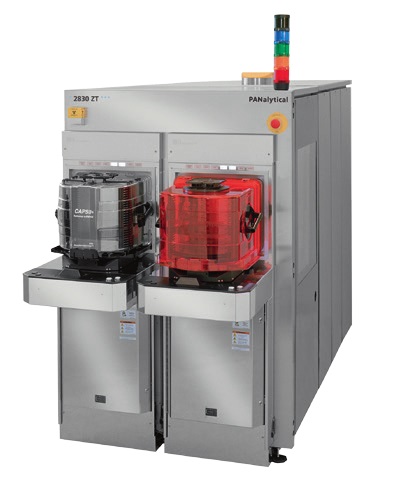
- XRF (2830 ZT) delivers thickness and composition information for a wide range of thin films, with contamination and dopant levels and surface uniformity on wafers up to 300mm in size
- XRD (X'Pert3 MRD and X'Pert3 MRD XL) provides absolute, calibration-free, and accurate information on crystal growth, giving material composition, film thickness, grading profile, and phase and crystal quality
- Gas analyzers from Servomex: Lowest level of ultra-trace O2 measurements & 1st choice in moisture analysis with the
DF500 and DF700 series. More info
- Particle counting from Particle Measuring Systems: Continuous particle counting sensitivity for chemicals, water, airborne, compressed gas, and molecular applications with the Ultra DI 20 Plus, Chem 20 and LASAIR III 110. More info
- 20 – 22 May: Semicon SEA Exhibition
- 23 May: XRD User Day
- 27 May Morning: Chemicals User Day
- 27 May Afternoon: Open Lab Day (see our total solutions from elemental, phase quantification, particle size, porosity measurement instruments and more)
- 28 May: XRF User Day
SEMICON SEA 2025
Cutting edge metrology solutions for the front end department
20 - 22 May, Marina Bay Sands Convention Center (Singapore)
Booth #L3142, Level 3, Cassia Room

Event
Semiconductor metrology refers to steps and practices that are being implemented in the area for the measurement and characterization of the physical and electrical properties of semiconductor devices and materials. Accurate dimensions and metrology determined by measurement results have been the key factors thus far for production processes with low tolerances and high performances. Malvern Panalytical offers a range of advanced x-ray metrology solutions, tools, and technologies developed with the goal of supporting various stages of semiconductor manufacturing with non-destructive measurements, from material characterization to wafer inspection.
Cutting-edge solutions for front-end departments
Talk by our expert scientist:
Talk to our experts. Bring your samples for analysis.
Malvern Panalytical is closely associated with the electronics industry with a wide range of solutions across the entire value chain:


We are proud to have sister companies, Servomex and Particle Measuring Systems join us at the booth.
You might also be interested in these events. Save the dates
facebook twitterrssinstagramlinkedinyoutube